Basic Info
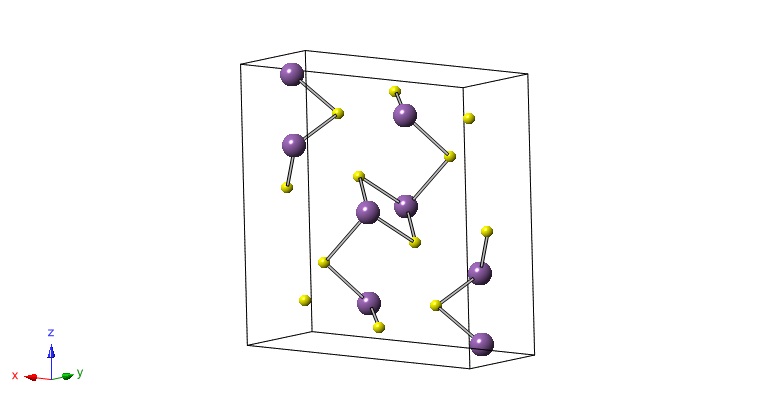
Bismuth trisulfide (Bi2S3) has an orthorhombic crystal structure with 4 molecules per unit cell. Each molecule contains two bismuth atoms and 3 sulfide atoms which add up to 20 atoms per unit cell. Bi2S3 occurs naturally in the form of bismuthinite, which has a lead-gray streaked color with a metallic luster. The mineral is primarily found in Bolvia, Peru, central Europe, Austrailia, and the western United States. Bismuthinite is mainly processed to obtain pure bismuth metal or other bismuth compounds, but has also been researched for the use in photovoltaics. 1
Crystal Structure
| Fractional Coordinates | Orthogonal Coordinates | |||||||
|---|---|---|---|---|---|---|---|---|
| Label | Elmt | x | y | z | xor[Å] | yor[Å] | zor[Å] | |
| 1. | T1 | Bi | 0.5165 | 0.2500 | 0.1748 | -3.914 | 2.533 | 4.141 |
| 2. | T1 | Bi | 0.9835 | 0.7500 | 0.6748 | -6.849 | 8.734 | 8.119 |
| 3. | T1 | Bi | 0.4835 | 0.7500 | 0.8252 | -2.532 | 9.931 | 4.286 |
| 4. | T1 | Bi | 0.0165 | 0.2500 | 0.3252 | 0.403 | 3.729 | 0.308 |
| 5. | T2 | Bi | 0.6596 | 0.7500 | 0.4655 | -3.971 | 6.133 | 6.169 |
| 6. | T2 | Bi | 0.8404 | 0.2500 | 0.9655 | -6.946 | 11.534 | 5.081 |
| 7. | T2 | Bi | 0.3404 | 0.2500 | 0.5345 | -2.475 | 6.331 | 2.258 |
| 8. | T2 | Bi | 0.1596 | 0.7500 | 0.0345 | 0.501 | 0.930 | 3.347 |
| 9. | T3 | S | 0.6230 | 0.7500 | 0.0575 | -3.543 | 1.609 | 6.617 |
| 10. | T3 | S | 0.8770 | 0.2500 | 0.5575 | -7.157 | 7.076 | 6.051 |
| 11. | T3 | S | 0.3770 | 0.2500 | 0.9425 | -2.902 | 10.855 | 1.810 |
| 12. | T3 | S | 0.1230 | 0.7500 | 0.4425 | 0.711 | 5.387 | 2.376 |
| 13. | T4 | S | 0.7153 | 0.2500 | 0.3063 | -5.681 | 4.163 | 5.333 |
| 14. | T4 | S | 0.7847 | 0.7500 | 0.8063 | -5.151 | 9.999 | 6.471 |
| 15. | T4 | S | 0.2847 | 0.7500 | 0.6937 | -0.764 | 8.301 | 3.095 |
| 16. | T4 | S | 0.2153 | 0.2500 | 0.1937 | -1.294 | 2.464 | 1.957 |
| 17. | T5 | S | 0.4508 | 0.7500 | 0.3730 | -2.127 | 4.923 | 4.839 |
| 18. | T5 | S | 0.0492 | 0.2500 | 0.8730 | -0.027 | 9.789 | -0.410 |
| 19. | T5 | S | 0.5492 | 0.2500 | 0.6270 | -4.319 | 7.540 | 3.589 |
| 20. | T5 | S | 0.9508 | 0.7500 | 0.1270 | -6.418 | 2.674 | 8.838 |
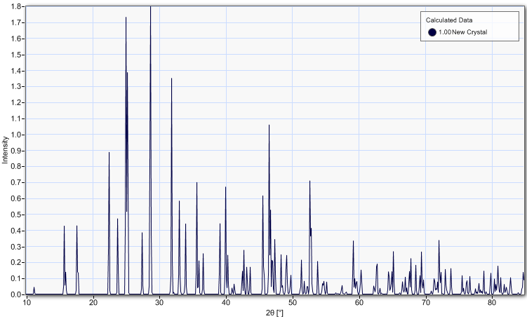
The graph below shows peak intensities for Bi2S3:
PV Applications
Bi2Si3 thin films are prepared from several methods which include: Cathodic electrodeposition, anodic electro deposition, vacuum evaporation, hotwall method, solution-gas interface, spray deposition, and chemical bath deposition. The most common method for Bi2Si3 prepared films is chemical bath deposition. This is because it is simple, economic, and well suited for a large area of any configuration. 2
Bi2Si3 thin films prepared from chemical bath deposition reach fill factors around 46.77% and a conversion efficiency of 0.089%. 3
Basic Parameters at 300 K
| Crystal structure: | Orthorhombic | 4 |
| Group of symmetry: | Pnma | 4 |
| Number of atoms in 1 cm3: | 3.99*1026 | 4 |
| Unit cell volume: | 501.6730 Å3 | 5 |
| Atoms per unit cell: | 20 | 4 |
| Density: | 6.807 g/cm3 | 4 |
| Dielectric constant: | ɛ(0)|| = 120 T=300K , at 1kHz | 5 |
| ɛ(0)⊥ = 38 T=300 K, E ⊥ c | ||
| ɛ(∞)|| = 13 T=300 K, E || c | ||
| ɛ(∞) ⊥ = 9 T=300, 90 K, E ⊥ c | ||
| Lattice constants: | a = 11.305 Å | 4 |
| b = 3.981 Å | ||
| c = 11.147 Å |
Band Structure and carrier concentration
Graph of carrier concentration may be found in 6
Donors and Acceptors
Impurities: Pb, Cu, Fe, As, Sb, Se, Te 7
Electrical Properties
Basic Parameters of Electrical Properties
| Energy gap: | 1.3 eV T=300 K, E ⊥ b: | 5 |
| 1.45 eV T=77 K, E ⊥ b | ||
| Intrinsic carrier concentration: : | n = 3 × 1018 cm-3 T = 300 K : | 5 |
| Carrier mobility: : | μn = 200 cm2/Vs T=300 K : | 5 |
| Hole mobility: : | μh = 1100 cm2/Vs : | 8 |
| Intrinsic resistivity: : | ρ = 105 Ω cm T=300K: | 2 |
| Electrical Conductivity: : | σ = 10-6…10-7 Ω-1 cm-1 T=300 K: | 5 |
Optical properties
Refractive indices:
λ = 589.3 nm 5
| nα | 1.315 |
| nβ | 1.900 |
| nγ | 1.670 |
Absorption coefficient: α = 104 cm-1 (In the order of) 2
Graph of optical transmittance data may be found in:9
Mechanical properties, elastic constants, lattice vibrations Basic Parameters
| Hardness: | 2-2.5 | 7 |
| Cleavage planes: | Perfect on (010) | 7 |
| Imperfect on (100), (110) | Ralph2003 |
Developed at the University of Utah primarily by undergraduate students Jeff Provost and Carina Hahn working with Prof. Mike Scarpulla. Caitlin Arndt, Christian Robert, Katie Furse, Jash Sayani, and Liz Lund also contributed. The work was fully supported by the US National Science Foundation under the Materials World Network program award 1008302. These pages are a work in progress and we solicit input from knowledgeable parties around the world for more accurate or additional information. Contact [email protected] with such suggestions.
- 1. Materials handbook: [foundation for the science of metallurgy; compares the advantages and disadvantages of different manufacturing processes; comprehensive in approach]. New York [u.a.]: {McGraw-Hill}, 2002.
- 2. a. b. c. «Chemical deposition of Bi2S3 thin films from thioacetamide bath», Materials Chemistry and Physics, т. 41, № 2, с. 98 - 103, 1995.
- 3. «Photoelectrochemical cells based on chemically deposited nanocrystalline Bi2S3 thin films», Materials Chemistry and Physics, т. 60, № 2, с. 196 - 203, 1999.
- 4. a. b. c. d. e. f. «First-principles study of the electronic properties of A2B3 minerals, with A=Bi,Sb and B=S,Se», Physics and Chemistry of Minerals, т. 32, № 4, с. 295 - 300, 2005.
- 5. a. b. c. d. e. f. g. Semiconductors Data Handbook. Berlin: Springer, 2004, с. 691.
- 6. Citekey Park2011 not found
- 7. a. b. c. «Bismuthinite». 2003.
- 8. «Bi2S3 as a high Z material for γ-ray detectors», IEEE Transactions on Nuclear Science, т. 22, № 1, с. 246 - 250, 1975.
- 9. «Structure and Composition of Chemically Deposited Thin Films of Bismuth Sulfide and Copper Sulfide Effect on Optical and Electrical Properties», Journal of The Electrochemical Society, т. 140, с. 754–759, 1993.